Green Photonics: High Power Quantum Well and Quantum Dot Lasers
Energy efficiency is one of the most important challenges of the 21st century. We are working to improve energy efficiency in industrial and other high power lasers.
In industrial lasers used for material forming, welding and cutting the benefits of energy efficiency are magnified through the higher powers and resulting quality of finish that can be achieved leading to improved products and enhanced competitiveness. In high power lasers used in medical applications (e.g. scalpel, photodynamic therapy) enhanced energy efficiency reduces cost of use and increases portability leading to increased uptake and local use (e.g. a G.P.’s surgery).
For either direct use or when laser diodes are used as pump sources the key and interrelated factors are maximum power output, efficiency of electrical to optical power conversion and beam quality. The maximum power output is limited when the detrimental effects, such as the increase in threshold current and decrease in efficiency due to self-heating, outweigh the beneficial effects with increasing current density (the resulting decrease in optical power with increasing current is known as thermal rollover). In some material systems catastrophic bulk or mirror damage (COBD or COMD) have become the major issues.
Activities
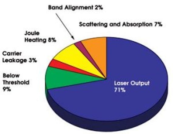
Spurred in part by funding from the US government under the DARPA “SHEDS” programme, in which Cardiff University participated as an external contractor, the so called “wall plug efficiency” (electrical to optical power conversion efficiency) of high power QW (Quantum Well) laser diodes has recently been improved to ~70% over a very limited wavelength range and at a specific output power. In the figure the factors that contribute to the electrical input power of the highest performance 970nm, high power laser bar are listed. Band alignment, Joule heating and carrier leakage are factors common to all semiconductor lasers and require special attention to the Ohmic contacts, the band alignment at hetero-junctions and doping levels; in recent work it is these factors that have been improved. The remaining factors are largely made up of the below threshold term and the scattering and absorption loss. The former term contains the parasitic spontaneous recombination and non-radiative recombination processes that occur in raising the carrier density high enough to achieve lasing.
Our work is targeted at reducing these contributions and in developing approaches to reduce COMD and COBD and maximising the transfer of optical power to the application.
One approach to maximising transfer of optical power is to match laser beam divergence to (for example) fibre beam collection and this usually requires a reduced device beam divergence as described below.
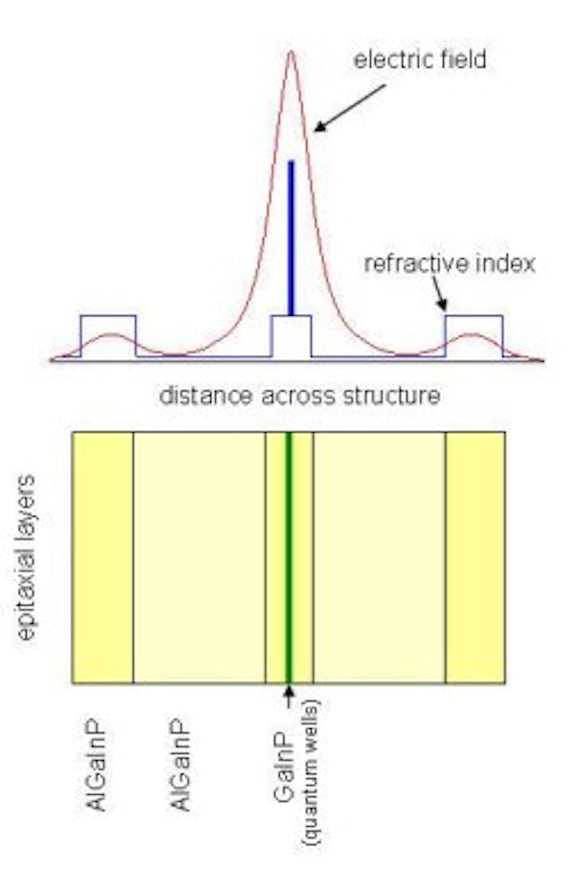
A narrow beam divergence can be achieved by careful design of the waveguiding epitaxial layers in a separate confinement heterostructure. A mode expansion layer structure enables the optical mode within the structure to be widened without significantly reducing the confinement factor (the fraction of the optical mode overlapping with the quantum wells and hence producing gain) - a normal consequence with other structures. A low confinement factor increases the threshold current - an undesirable effect. The effect on the farfield divergences of varying the widths, spacings and compositions of the layers is modelled using in-house developed software based on the transfer function method. Wafers of the resulting designs (grown by IQE (Europe) Ltd) are fabricated into laser diodes and characterised, with particular emphasis on the farfield divergence and threshold current. The beam divergence has successfully reduced to 18 degrees (full width half maximum) and subsequently below 14 degrees.
The light intensity is related to the electric field which is governed by Maxwell's equations, and tends to be higher in regions of higher refractive index. The high refractive index mode expansion layers at the sides widen the extent of the electric field, which when Fourier transformed gives a narrower beam divergence. By adjusting the position and thickness of the layers the desired characteristics can be achieved.
Publications
- Sobiesierski, A. and Smowton, P. M. 2011. Quantum-dot lasers: physics and applications. In: Bhattacharya, P. , Fornari, R. and Kamimura, H. eds. Comprehensive Semiconductor Science and Technology: Volume 6: Devices and Applications. Burlington, VT: Elsevier. , pp.353-384. (10.1016/B978-0-44-453153-7.00034-1)
- Elliott, S. et al. 2010. Time resolved studies of catastrophic optical mirror damage in red-emitting laser diodes. Journal of Applied Physics 107 (12) 123116. (10.1063/1.3437395)
- Elliott, S. , Berry, G. and Smowton, P. M. 2006. Optimisation of high power AlGaInP laser diodes for optical storage applications. IEE Proceedings Optoelectronics 153 (6), pp.321-325. (10.1049/ip-opt:20060050)