Advanced Superlattice Infrared detectors for Space Application (ASISA)
The objective of this project is to demonstrate Type-II InAs/GaSb superlattice (T2SL) infrared photodetectors with high performance (low dark-current, high quantum efficiency) for space applications.
Thanks to its unique properties, using this material as the absorption region of a photodetector has proven to be a successful approach in the mid wavelength (λ = 3 - 5 μm) and long wavelength (λ = 8 - 12 μm) infrared spectral domain. However, addressing the far infrared (VLWIR, λ > 12 μm), required for most applications in space, is a new challenge to outperform the current state-of-the-art in this technologically important spectral regime.
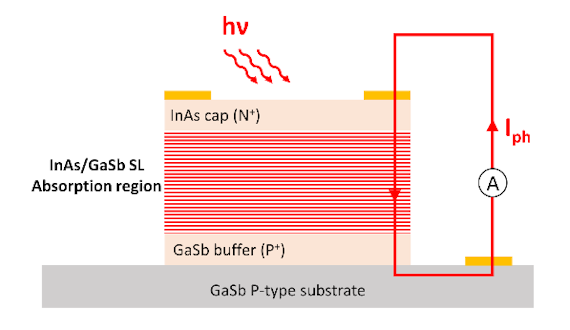
The T2SL material is a periodic structure of alternating nanometer-scaled layers of InAs and GaSb. The period composition and thickness can be precisely controlled during Molecular Beam Epitaxy growth. The material quality is evaluated using high resolution X-ray diffraction, atomic force microscopy and photoluminescence measurements. Circular mesa photodiodes are then fabricated using standard photolithography and etching procedures.
To characterise the device performances, we have access to state-of-art equipment such as a Keysight B1500A Semiconductor Device Analyzer, a Lakeshore TTPX cryogenic probe station and a Thermo Scientific Nicolet iS50R FT-IR spectrometer.

Funding
This project has received funding from the European Union’s Horizon 2020 research and innovation programme under the Marie Skłodowska-Curie grant agreement No. 743521.