CSC concludes pioneering VCSEL project
25 January 2019
A consortium led by the Compound Semiconductor Centre (CSC) has concluded an Innovate UK-funded project to produce cheaper, faster devices that will drive tomorrow’s sensing technologies.
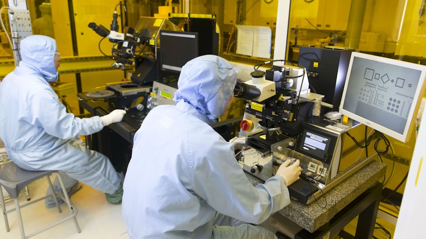
CSC, a Cardiff University partnership with IQE plc, has been working with SPTS Technologies Ltd - an Orbotech company – and scientists at Cardiff and Swansea Universities to develop Vertical-Cavity Surface-Emitting Lasers (VCSELs) used in smart phone facial recognition, 3D imaging and laser range-finding.
VCSELS are semiconductor laser chips that emit laser light from the top surface of the chip, rather than the edge, allowing tens of thousands of tiny lasers to be manufactured on a single wafer of semiconductor material in a simplified process. They can be tested on-wafer during the production process, resulting in lower fabrication costs compared to other laser technologies.
The CSC project - ‘High Efficiency Manufacturing of Vertical Cavity Surface Emitting Lasers (VCSELs)’ - has delivered key process modules that will enable the industry to transition from small-diameter manufacturing processes, currently used for VCSELs, up to a high-uniformity 150mm (six inch) semiconductor wafer platform.
Dr Wyn Meredith, Director of CSC said: “The HEMAN project has played a crucial role in allowing us to exploit the benefits of scale-up productivity. Processing one 150mm (six inch) wafer delivers far more devices than a 75mm (three inch) wafer."
This will drive a step change in cost reduction for VCSELs, and thus their adoption in mass-market applications such as 3D imaging, proximity sensing, range-finding and light detection and ranging (LiDAR), used in autonomous vehicles.
CSC’s work included the commissioning of a custom 150mm oxidation tool at the ERDF-funded Institute for Compound Semiconductors which is used for a particularly challenging stage of preferential oxidation of aluminium-rich layers in the VCSEL layer structure.
The 150mm VCSEL prototyping capacity leveraged by the consortium will combine with device-scale optimization and validation of VCSEL epitaxial materials to form a core research and manufacturing competence in the CSConnected Compound Semiconductor cluster in South Wales.
The full story can be found here on the Compound Semi Conductor Centre website.
And CSC has been awarded Welsh Government project backing through the SMARTCymru scheme via the European Regional Development Fund (ERDF).
The funding will support a technical and commercial feasibility study for a CSC project to develop a vertical Gallium Nitride device manufacturing capability within the UK.
Industry analysts forecast the GaN power market will grow rapidly over the next five years, creating excellent opportunities for innovative new products to unlock growth potential.
Vertical GaN has been identified as a suitable technology for lower voltage, lower power automotive applications including on board battery charging for hybrid and electric vehicles.
The full story can be found here on the Compound Semi Conductor Centre website.
Share this story

The institute provides cutting-edge facilities to help researchers and industry work together.


